| Sign In | Join Free | My portofva.com |
|
| Sign In | Join Free | My portofva.com |
|
| Categories | Fused Quartz Plate |
|---|---|
| Brand Name: | ZMSH |
| Model Number: | 6 Inch Quartz Wafer |
| Certification: | rohs |
| Place of Origin: | CHINA |
| MOQ: | 10 |
| Price: | by case |
| Payment Terms: | T/T |
| Supply Ability: | 1000pcs per month |
| Delivery Time: | 5-8weeks |
| Packaging Details: | Package in 100-grade cleaning room |
| Diameter: | 6 inch (150mm) |
| Thickness Tolerance: | ±0.02mm |
| Total Thickness Variation: | ≤10μm |
| Surface Roughness: | ≤0.5nm Ra |
| Parallelism: | ≤3μm |
| Resistivity: | >10¹⁶ Ω·cm |
| Company Info. |
| SHANGHAI FAMOUS TRADE CO.,LTD |
| Verified Supplier |
| View Contact Details |
| Product List |
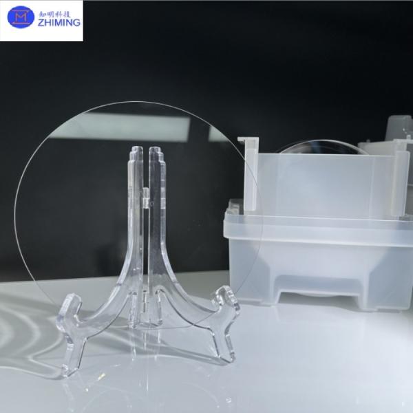
The 6-inch quartz wafer (150mm diameter) is fabricated from high-purity quartz glass (purity ≥99.999%) with thickness ranging from 50-500μm. Surface roughness is controlled to Ra ≤0.5nm through CMP (Chemical Mechanical Polishing). The manufacturing process includes:
· Raw Material Purification: Extraction of electronic-grade silicon from quartz sand via chlorination and reduction processes, achieving 99.9999% purity.
· Single-Crystal Growth: Cultivation of single-crystal silicon rods using the Czochralski (CZ) method, with defect density <1 defect/cm².
· Cutting and Processing: Slicing silicon rods into 150mm wafers via multi-wire sawing, followed by double-sided polishing and laser etching to ensure thickness tolerance ≤±15μm.
| Parameter | Specification |
| Diameter | 6 inch (150mm) |
| Thickness Range | 0.5mm~3.0mm |
| Thickness Tolerance | ±0.02mm |
| Total Thickness Variation | ≤10μm |
| Surface Roughness (Polished) | ≤0.5nm Ra |
| Parallelism | ≤3μm |
| CTE (20-300°C) | 0.55×10⁻⁶/°C |
| Transmittance @193nm | >92% |
| Resistivity | >10¹⁶ Ω·cm |
| Vacuum Compatibility | 10⁻¹⁰ Torr |
| Flexural Strength (Strengthened) | 500-700MPa |
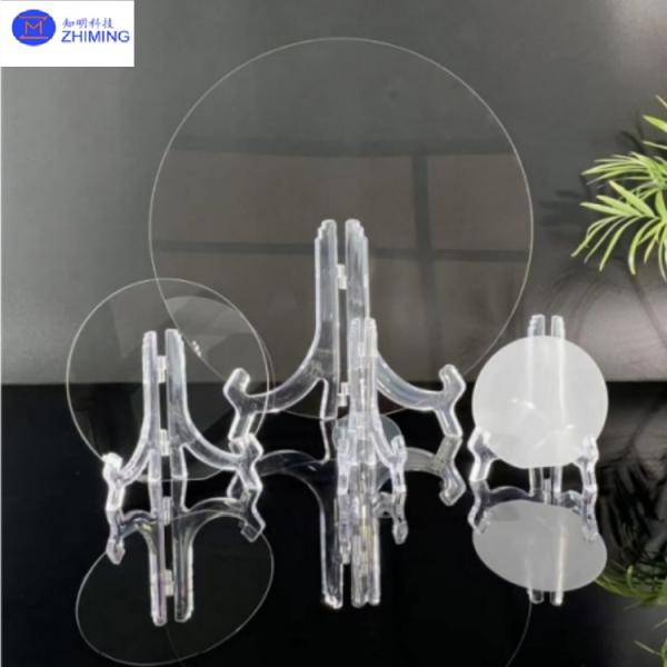
The 6-inch quartz wafer is a circular thin film made of high-purity quartz material, widely used in semiconductor manufacturing, optoelectronics, and precision optics. Key features include:
· High Purity and Thermal Resistance: Quartz glass purity ≥99.999%, softening point ~1730°C, short-term tolerance up to 1450°C.
· Low Thermal Expansion: Thermal expansion coefficient 0.5×10⁻⁶/°C (25-300°C), capable of withstanding thermal shock (ΔT ≥800°C).
· Chemical Stability: Resists corrosion from all acids except hydrofluoric acid, with corrosion resistance 30× higher than ceramics and 150× higher than stainless steel.
· Optical Performance: High transmittance in the ultraviolet to near-infrared spectrum (visible light >93%, near-infrared >95%).
· Mechanical Strength: Mohs hardness of 7, compressive strength superior to standard glass.

1. Semiconductor Manufacturing: Used in diodes, transistors, and MOSFETs, supporting automotive electronics and power semiconductors.
2. Optoelectronics: Serves as substrates for optical fibers, laser devices, and waveguides in 5G networks and data centers.
3. Precision Optics: Applied in infrared imaging systems, laser optics, and high-transmittance lenses.
4. Sensors and Instruments: Core components in MEMS sensors and medical diagnostic equipment.
5. Aerospace: High-temperature optical windows and heat-resistant components for spacecraft.
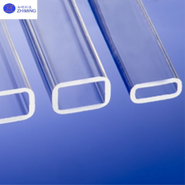
Quartz tubes are high-purity quartz glass fabricated into tubular structures, widely used in semiconductor diffusion/oxidation processes and photovoltaic equipment. Our services include:
· Custom Processing: Inner diameters (5-50mm), lengths (100-1000mm), and wall thicknesses (0.5-3mm). Complex geometries (bent, multi-chamber tubes) are supported.
· Technical Advantages: Operates at 1100°C long-term, low hydroxyl content (<1ppm), and high contamination resistance, meeting semiconductor-grade cleanliness requirements.

1. Q: What are the primary applications of 6-inch quartz wafers?
A: 6-inch quartz wafers are widely used in semiconductor manufacturing (e.g., diodes, MOSFETs), optoelectronics (fiber optics, lasers), and precision sensors due to their high thermal stability and optical transparency .
2. Q: What challenges exist in 6-inch quartz wafer production?
A: Key challenges include maintaining ultra-high purity (>99.999% SiO₂), minimizing defects during crystal growth, and ensuring uniformity in slicing/polishing processes .
Tags: #6 Inch Quartz Substrate, #Customized, #Fused Silica Plates, #SiO₂ Crystal, #Quartz wafers, #JGS1/JGS2 Grade, # High-Purity, #Fused Silica Optical Components, #Quartz Glass Plate, #Diameter 150mm, #Quartz Crystal Glass Wafer, #5N Purity SiO₂, #Heat-Resistant, #Transparent, #Monocrystalline Quartz Crystal Substrate, #SAW Devices
|
